Privacy statement: Your privacy is very important to Us. Our company promises not to disclose your personal information to any external company with out your explicit permission.
Select Language
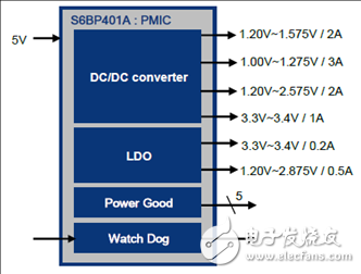
Cypress's S6BP401A is a Power Management Integrated Circuit (PMIC) that includes four buck 2.1MHz DC/DC converters with built-in switching FETs, two low dropout (LDO) regulators and digital window watchdog timing The .VIN input voltage is 4.5V-5.5V, and the built-in switching FET has a current of up to 3A. It is mainly used in automotive applications, advanced driver assistance systems (ADAS), camera systems such as security cameras and industrial applications. This article introduces the main features of S6BP401A, block diagram and architecture block diagram, typical application circuit, and evaluation board S6SBP401AJ0SA1001 main indicators, circuit diagram, bill of materials and PCB design.
S6BP401A is a power management IC, consists of quad buck 2.1 MHz DC/DC converter with built-in switching FETs, dual LowDrop-out regulator (LDOs) and a digital windowed watchdog TImer. Having the switching FETs built-in, S6BP401A realizes highpower The internal FETs are capable to handle up to 3A load. AsS6BP401A employs the current mode architecture, it has fast load transient response. Built-in output voltage setTIng resistors andcompensaTIon circuits reduce BOM cost and Component area.
Main features of S6BP401A:
Quad Buck DC/DC Converter (DD1 to DD4)
VIN Input Range: 4.5V to 5.5V
Switching Frequency
External clock mode: 1.8 MHz to 2.4 MHz
Internal clock mode: 2.0 MHz to 2.2 MHz
Built-in Switching FETs up to 3A
Built-in Output Voltage SetTIng Resistors
Built-in Compensation Circuits
Dual LDO (LD1, LD2)
VIN Input Voltage Range: 2.97V to 5.5V
Built-in Output Voltage Setting resistors
Power Good Monitor Output for each DC/DC Converters, LDOs
Built-in Windowed Watchdog Timer (WDT)


Figure 3. Typical application circuit for S6BP401A
Evaluation Board S6SBP401AJ0SA1001
S6SBP401AJ0SA1001 and S6SBP401AM2SA1001 are the evaluation kit for power block of automotive ADAS platform.
The board implements power management IC S6BP401A.

![[Original] Cypress S6BP401A Automotive ADAS Power Management Solution](http://i.bosscdn.com/blog/12/1P/64/504_0.png)
![[Original] Cypress S6BP401A Automotive ADAS Power Management Solution](http://i.bosscdn.com/blog/12/1Z/1B/11_0.png)
![[Original] Cypress S6BP401A Automotive ADAS Power Management Solution](http://i.bosscdn.com/blog/12/20/01/2E7_0.png)
Figure 6. Circuit diagram of the evaluation board S6SBP401AJ0SA1001
Evaluation Board S6SBP401AJ0SA1001 Bill of Materials:
![[Original] Cypress S6BP401A Automotive ADAS Power Management Solution](http://i.bosscdn.com/blog/12/21/01/2211_0.png)
![[Original] Cypress S6BP401A Automotive ADAS Power Management Solution](http://i.bosscdn.com/blog/12/22/02/5F4_0.png)


इस आपूर्तिकर्ता को ईमेल

Privacy statement: Your privacy is very important to Us. Our company promises not to disclose your personal information to any external company with out your explicit permission.

Fill in more information so that we can get in touch with you faster
Privacy statement: Your privacy is very important to Us. Our company promises not to disclose your personal information to any external company with out your explicit permission.